ASML, the leader in semiconductor equipment, helps wafer foundries realize advanced process technology, and each generation of its equipment means the cutting-edge moment of each generation of technology. "Science and Technology News" has also sorted out some of ASML's most classic equipment in the past, taking readers back to every critical moment in chip shrinkage.
The evergreen tree of photolithography machines: PAS 5500The most classic equipment to mention is the stepper scanning system PAS 5500, launched in 1991, which is still in service in the wafer fab 34 years ago.
In addition to being one of the longest-lasting and most functional lithography platforms in the company's history, it is also the key to ASML's rapid success in the market. In fact, before the advent of this device, ASML ranked third in the photolithography market, far behind the two giants at the time, Nikon and Canon. However, it was a great success after its launch, and quickly jumped to second place, and also laid the foundation for becoming the world's leader in photolithography technology.
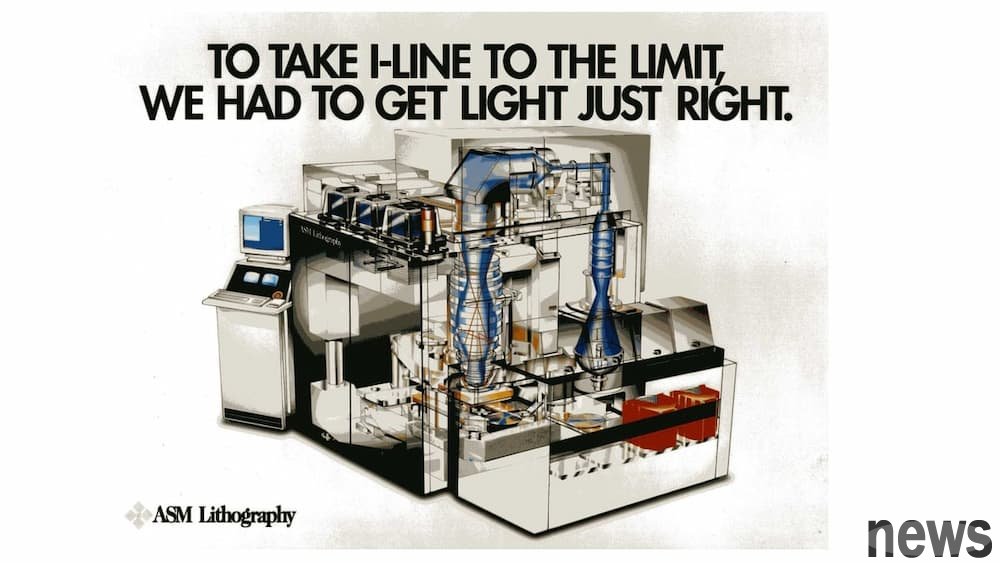
▲ Early advertising of the PAS 5500 platform. (Source: ASML)
As for why it’s called “PAS”? In fact, this is from a series of equipment pioneered by Philips researchers in the 1970s. The full name of the PAS 5500, "the Philips Automatic Stepper" (PAS), mainly commemorates the origin of this machine and also represents the long-term cooperative relationship between ASML and Philips.
ASML also introduced that after more than 30 years, each PAS system has its own unique story, and it spans different generations with different semiconductor industries. For example, in 2021, the PAS 5500/275 system, which had been in service for 25 years, was refurbished and sold after being engaged in the production of memory and radio frequency (RF) modules, and was converted into front-line production of virtual reality (VR).
ASML pointed out that although PAS 5500 has been retired from the most advanced processes, it still has great advantages in the second-hand market because of its low cost, small size, simplicity and stability. The company has also refurbished and resold more than 500 PAS 5500 systems. At the same time, in order to continue to support customers who use this machine, ASML also stated that the life cycle of this product has been successfully extended to 2035.
The world's first and so far only "dual wafer platform" exposure equipment: TWINSCANThen in 2001, ASML launched TWINSCAN equipment, a breakthrough "dual wafer platform" technology that can move two wafers at the same time and alternately perform lithography and measurement functions.
The emergence of TWINSCAN has helped customers achieve a huge leap in the production process. ASML exposure scanning position measurement system expert Bert van der Pasch recalled, "TWINSCAN's new technology is limited, but what is truly revolutionary is the exchange of the two platforms. Many parts are normal upgrades, but the design of the wafer exchange platform is completely different, and we have to make it work."

▲ ASML exposure scanning position measurement system expert Bert van der Pasch. (Source: ASML)
TWINSCAN is the world’s first and still the only exposure system platform with dual wafer carrier modules. From a current perspective, wafers are alternately loaded into two platform modules. The wafer on the right can be exposed to extreme ultraviolet light (EUV) to engrave the circuit design image (Pattern) on the wafer. The wafer on the left is simultaneously optimized for accuracy (Alignment) by the machine's measurement instruments. The two platforms alternately perform lithography and measurement functions to maximize the productivity and yield of the equipment.
The TWINSCAN equipment model launched in 2001 is TWINSCAN AT:750T. It is a KrF exposure system with a light source wavelength of 248 nanometers and is mainly designed for the 130 nanometer process. Then in 2003, ASML launched the TWINSCAN AT:1150i equipment, which became the first exposure machine to use immersion lithography. By 2006, the updated TWINSCAN
▲ The ASML engineering team celebrates the launch of TWINSCAN XT:1700i. (Source: ASML)
TWINSCAN platform is upgraded again, becoming the fastest: TWINSCAN NXTWhen entering the 2000s, wafer manufacturers found the limits of exposure resolution using immersion ArF systems, so ASML began to develop new EUV light sources. At the same time, the industry is also simultaneously exploring "double patterning" and "multiple patterning" methods.
However, double exposure means that twice the exposure steps are required, and the two layers of patterns must be aligned extremely accurately. If this technology is to be feasible in terms of cost and production, the speed and accuracy of the exposure system must be improved. So this also leads to the next major upgrade of TWINSCAN, which is the TWINSCAN NXT platform.
The TWINSCAN NXT platform adopts a newly designed and lighter wafer carrier, which greatly improves speed and performance. Bert also said, "While we are developing NXT, we are also simultaneously developing the next generation of systems using new EUV light sources."
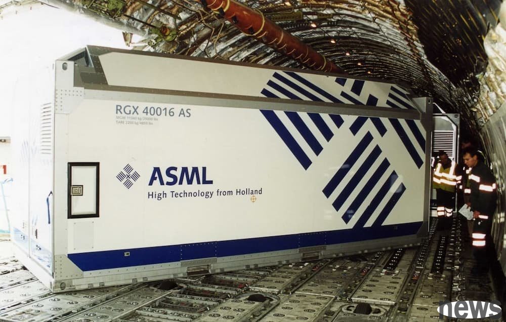
▲ ASML ships one of the first TWINSCAN systems. (Source: ASML)
The first NXT system, named TWINSCAN NXT:1950i, was officially launched in 2008, helping to increase production efficiency by 30%, reaching a processing capacity of more than 200 wafers per hour, while increasing the overlay accuracy (Overlay) to 2.5 nanometers (nm).
The traditional TWINSCAN stage uses pneumatic levitation technology, allowing the stage to be suspended on a flat backplane. Therefore, the stage can float without friction and move independently during exposure scanning; the upgraded TWINSCAN NXT system uses magnetic levitation to support the stage.
According to ASML’s latest sharing, today’s TWINSCAN NXT moves two wafers at the same time electromagnetically, and can accelerate to 7G without friction, that is, 0 to 100km/h only takes about 0.4 seconds, allowing both accuracy and production speed to be taken into account during mass production of wafers.
ASML subsequently decided to expand the NXT platform to "dry technologies" (dry technologies), and launched the first dry exposure system TWINSCAN NXT:1470 in 2020, becoming the world's first exposure machine that can process more than 300 wafers per hour.
ASML’s biggest moat: EUVAccording to the official website, to push EUV technology to large-scale mass production, ASML spent more than 40 years, invested billions of dollars in R&D funds, and executed a key acquisition, which was the purchase of Cymer, a light source technology company.
ASML stated that after decades of research and development, it finally had the results of "first light". In 2006, ASML launched the first EUV alpha testing machine. At that time, it took 23 hours to expose a wafer. It was a breakthrough for research institutions such as IMEC, but it was almost impossible for mass production. By 2008, ASML produced the world's first batch of full-field EUV test wafers. The following year, it opened a workspace for EUV development and mass production at its headquarters in the Netherlands.
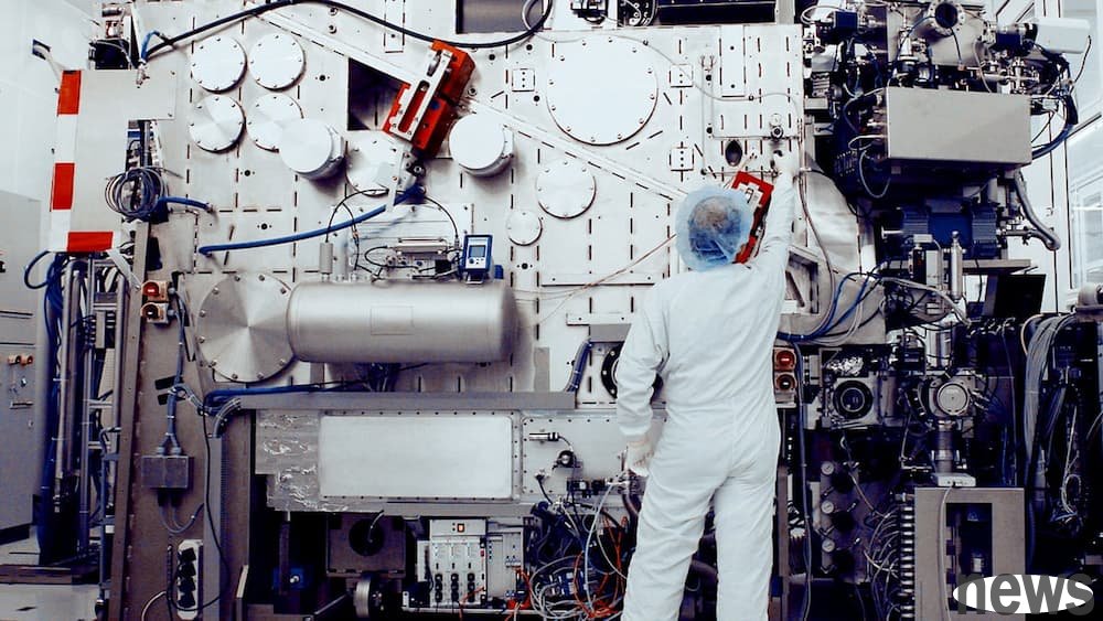
▲ One of ASML’s EUV prototype systems, also known as the “alpha test machine”. (Source: ASML)
In 2010, the first TWINSCAN NXE:3100 (EUV pre-mass production system) was shipped to the Samsung R&D Center in South Korea and was put into use for the first time on Christmas Eve.
ASML Executive Vice President of Technology Jos Benschop recalled, "We started working on this project in 1997. Suddenly, in 2010, you flew to South Korea, took a long taxi, changed your clothes, walked into the fab, turned a corner, and that machine was in front of you. It was a great moment. The original dream finally came true in the customer's factory."
By 2012, ASML’s major customers TSMC, Samsung, and Intel all agreed to participate in EUV research and development over a five-year period as part of the Customer Co-Investment Program in exchange for company shares. Subsequently, the first EUV mass production system TWINSCAN NXE:3300 was shipped in 2013, symbolizing another major step forward in the research and development of this new technology.
Looking back on the whole process, Jos smiled and said: "It took longer and was more difficult than I imagined. You can say that we are either very smart or very stubborn."
▲ ASML celebrates the shipment of the first EUV exposure machine in 2010. (Source: ASML)
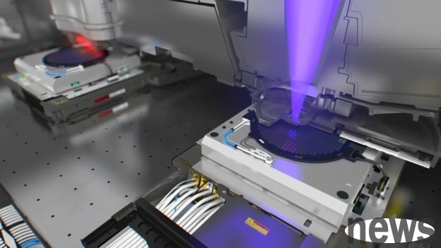
High-NA EUV is critical in the Amy era: TWINSCAN EXEAs wafers continue to shrink, ASML has increased the numerical aperture (NA) of EUV exposure machines from 0.33 to 0.55. Jos said that because this new lens is completely different from the past, new manufacturing and measurement methods must be proposed. At present, the first batch of High-NA EUV exposure machine TWINSCAN EXE:5000 has been shipped to customers at the end of 2023, and is expected to be put into high-volume production in 2025.
In fact, at all stages of EUV technology research and development, the most critical thing is transnational cooperation. Currently, ASML has successfully established and mobilized a global ecosystem to industrialize technology that many people thought was impossible, and will now push this technology into mass production.
Three decades of PAS 5500 TWINSCAN: 20 years of lithography innovation EUV lithography systems Making EUV: from lab to fab Further reading: ASML is actually the "three brothers"! A story of separation, unexpectedly rewriting the global semiconductor equipment landscape